


.png)


All pictures are for illustrative purposes only.
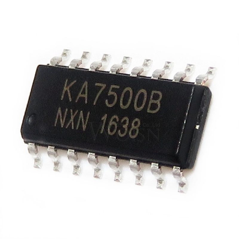
The KA7500B is used for the control circuit of the PWM switching regulator. The KA7500B consists of a 5V reference voltage circuit, two error amplifiers, a flip flop, an output control circuit, a PWM comparator, a dead time comparator and an oscillator. This device can be operated in the switching frequency of 1kHz to 300kHz.
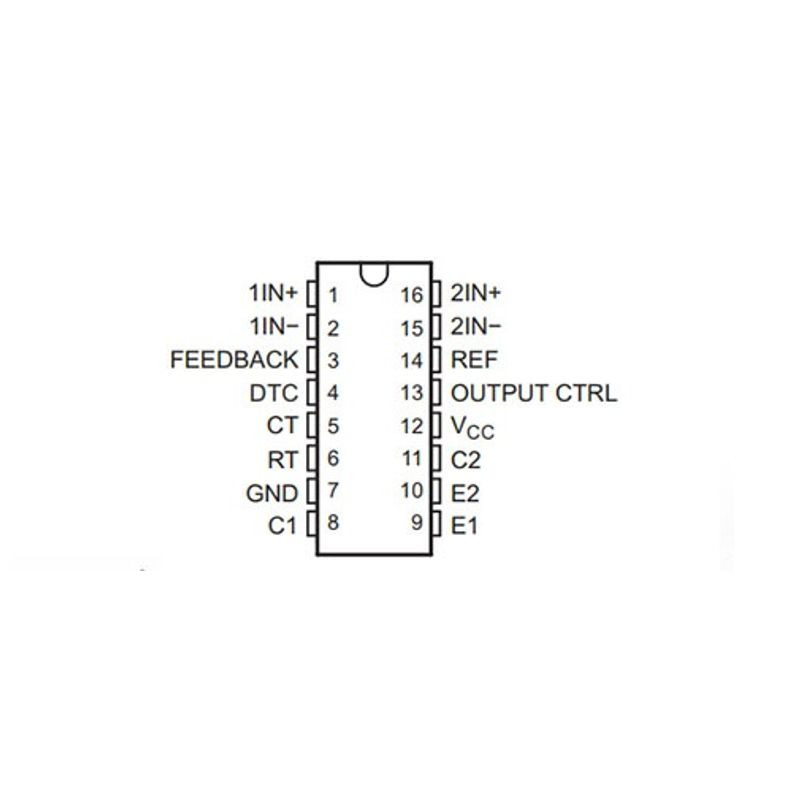
| Pin Number | Pin Name | Description |
| 1 | 1IN+ | The non-inverting input terminal of error amplifier 1. In the closed-loop system, the given signal of the controlled quantity will be input to the error amplifier through this pin, while in the open-loop system, the pin needs to be grounded or left floating. |
| 2 | 1IN- | The inverting input terminal of the error amplifier 1. In the closed-loop system, the feedback signal of the controlled quantity will be input into the error amplifier through this pin. At this time, it is also necessary to connect the feedback network between this pin and pin 3. In the open-loop system, this pin is grounded or left floating. |
| 3 | FEEDBACK | Feedback/PWM comparator input terminal. In a closed-loop system, different types of feedback networks can be connected between this pin and pin 2 as required to form various types of regulators such as proportional, proportional-integral, and integral to meet different user needs. |
| 4 | DTC | The dead time controls the output of the comparator. This terminal is used to set the value of TL494 dead time. When this pin is grounded, the dead time is the smallest, and the maximum station-to-empty ratio can be obtained. |
| 5 | CT | Oscillator timing capacitor access terminal. The value range of CT is usually between 0.001 and 0.1yF. |
| 6 | RT | Oscillator timing resistor access terminal. The value range of the foot is usually between 5 to 100kQ. |
| 7 | GND | Signal ground (reference ground for chip work). |
| 8 | C1 | The collector terminal of the output transistor VT1, which is the positive pulse output terminal. In push-pull working mode, this terminal outputs a positive pulse signal, and pin 11 outputs a negative pulse signal. The phase difference between the two is 1800. After isolation and amplification, the switching tube is driven separately. In single-ended working mode, this terminal can be connected in parallel with pin 11 to improve the output capability of the pulse width modulation controller TL494. |
| 9 | E1 | The emitter terminal of the output transistor VT1, this terminal is the reference ground terminal of the pin 8 output pulse signal and is generally directly connected to pin 7. |
| 10 | E2 | The emitter terminal of the output transistor VT2, this terminal is the reference ground terminal of the pin 11 output pulse signal and is generally directly connected to pin 7. |
| 11 | C2 | The collector terminal of the output transistor VT2, which is the reverse pulse output terminal. In the push-pull working mode, this terminal outputs a reverse pulse signal, and pin 8 outputs a forward pulse signal. The phase difference between the two is 1800. After isolation and amplification, they drive the switch tubes respectively. In single-ended working mode, this terminal can be connected in parallel with pin 8 to improve the output capability of the pulse width modulation controller TL494. |
| 12 | Vcc | Bias power (chip working power) access terminal. In application, a filter capacitor with a capacity of 0.1UF or more must be connected to the common ground terminal. |
| 13 | OUTPUT CTRL | Output working mode control terminal. Push-pull or single-ended output mode can be selected through this pin. When the terminal is connected to a high level, TL494 will work in push-pull mode, and the maximum duty cycle can reach 48% at this time. When the terminal is connected to a low level, the two output pulses are exactly the same, and the maximum duty cycle can reach 96%. |
| 14 | REF | The input current of the reference power supply output can reach 10mA. |
| 15 | 2IN- | The inverted input terminal of the error amplifier 2. This terminal can be connected to the feedback signal of the protection circuit to realize fault protection such as over-current and over-voltage. |
| 16 | 2IN+ | The non-inverting input terminal of error amplifier 2. This terminal is the protection threshold voltage (current) setting terminal, which is used to realize fault protection such as overcurrent and overvoltage. |