


.png)


All pictures are for illustrative purposes only.
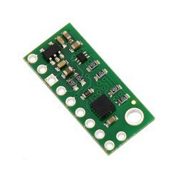
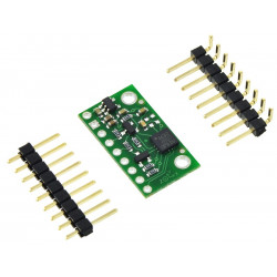
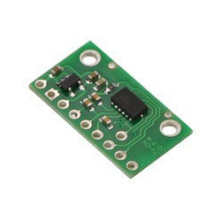
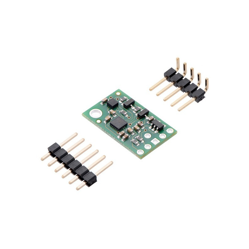
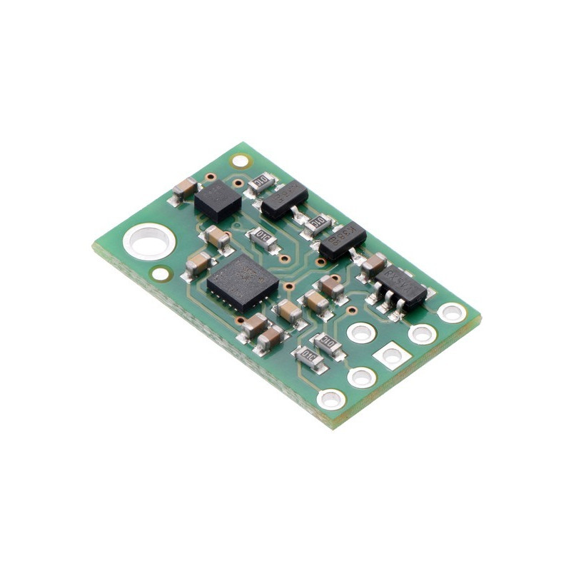
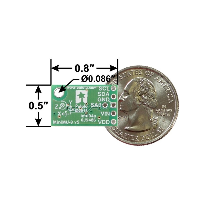
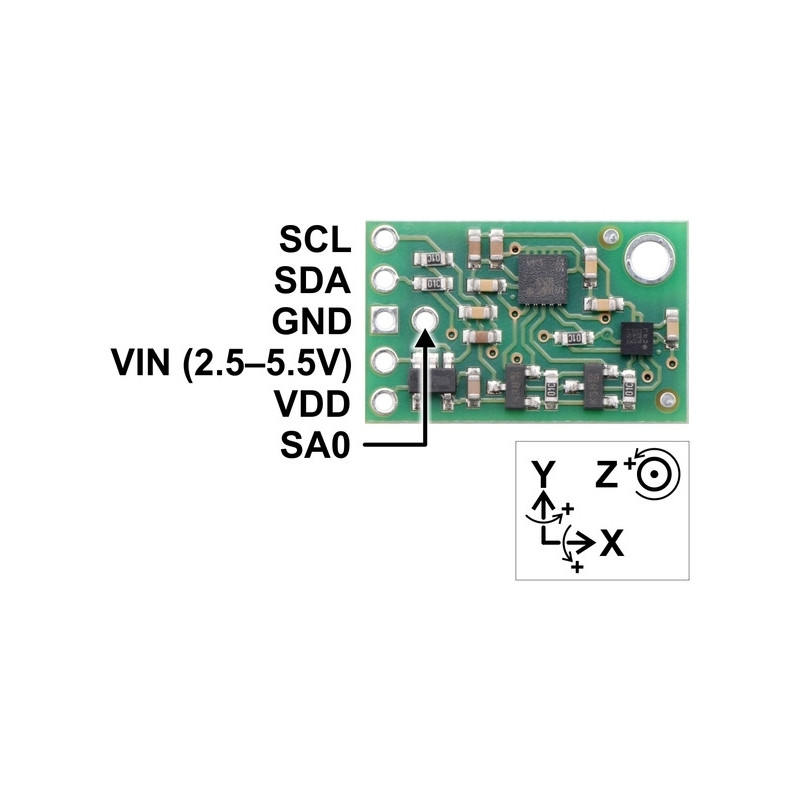
The Pololu MinIMU-9 v5 is an inertial measurement unit (IMU) that packs an LSM6DS33 3-axis gyro and 3-axis accelerometer and an LIS3MDL 3-axis magnetometer onto a tiny 0.8″ × 0.5″ board. An I²C interface accesses nine independent rotation, acceleration, and magnetic measurements that can be used to calculate the sensor’s absolute orientation. The MinIMU-9 v5 board includes a voltage regulator and a level-shifting circuit that allow operation from 2.5 to 5.5 V, and the 0.1″ pin spacing makes it easy to use with standard solderless breadboards and 0.1″ perfboards.
| Size: | 0.8″ × 0.5″ × 0.1″1 |
|---|---|
| Weight: | 0.7 g1 |
| Interface: | I²C |
|---|---|
| Minimum operating voltage: | 2.5 V |
| Maximum operating voltage: | 5.5 V |
| Axes: | pitch (x), roll (y), and yaw (z) |
| Measurement range: | ±125, ±245, ±500, ±1000, or ±2000°/s (gyro) ±2, ±4, ±8, or ±16 g (accelerometer) ±4, ±8, ±12, or ±16 gauss (magnetometer)2 |
| Supply current: | 5 mA |
| PCB dev codes: | imu04a |
|---|---|
| Other PCB markings: | 0J9486 |
| PIN | Description |
|---|---|
| SCL | Level-shifted I²C clock line: HIGH is VIN, LOW is 0 V |
| SDA | Level-shifted I²C data line: HIGH is VIN, LOW is 0 V |
| GND | The ground (0 V) connection for your power supply. Your I²C control source must also share a common ground with this board. |
| VIN | This is the main 2.5 V to 5.5 V power supply connection. The SCL and SDA level shifters pull the I²C bus high bits up to this level. |
| VDD | 3.3 V regulator output or low-voltage logic power supply, depending on VIN. When VIN is supplied and greater than 3.3 V, VDD is a regulated 3.3 V output that can supply up to approximately 150 mA to external components. Alternatively, when interfacing with a 2.5 V to 3.3 V system, VIN can be left disconnected and power can be supplied directly to VDD. Never supply voltage to VDD when VIN is connected, and never supply more than 3.6 V to VDD. |
| SA0 | 3.3V-logic-level input to determine I²C slave addresses of the two ICs (see below). It is pulled high by default through 10 kΩ resistor. This pin is not level-shifted and is not 5V-tolerant. |