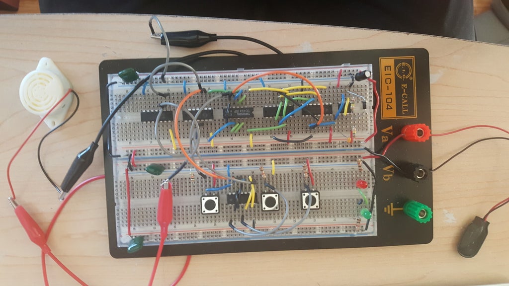
Blog navigation

Latest posts

2067 Views
Picture of IC Egg Timer

Created by: Gabriel Chiu

Overview

This project demonstrates the basics of digital logic, the characteristics of a NE555 timer, and demonstrates how binary numbers are counted. The components used are: a NE555 timer, a 12-bit ripple counter, two 2-input NOR gates, a 4-input AND gate, a 2-input AND gate, and a 2-input OR gate. The logic gates, NOR, AND, and OR come in TTL and CMOS equivalents which can be found at Lee’s Electronic. This project is a simple egg timer with two settings: hard or soft boiled and comes with a reset function.

Parts and Tools

  • 1x Breadboard (Lee’s Number: 10516)
  • 1x 9V battery (Lee’s Number: 8775, or 16123)
    • NOTE: THIS CIRCUIT CAN ALSO WORK USING 5V POWER. DO NOT EXCEED 9V BECAUSE IT MAY DAMAGE THE IC CHIPS
  • 1x 9V battery holder (Lee’s Number: 657 or 6538 or 653)
  • Solid hook-up wire (Lee’s Number: 2249)
  • Jumper Wire (Lee’s Number: 10318 or 21805)
  • Alligator Test Leads (Lee’s Number: 690)
  • 3x Tactile Switches (Lee’s Number: 31241 or 31242)
  • 1x NE555 Timer (Lee’s Number: 7307)
  • 1x 12-bit ripple counter CMOS 4040 (Lee’s Number: 7210)
  • 1x Dual Quad input AND gate CMOS 4082 (Lee’s Number: 7230)
  • 1x Quad 2-input AND gate CMOS 4081 (Lee’s Number: 7229)
  • 2x Quad 2-input NOR gate CMOS 4001 or 74HC02 (Lee’s Number: 7188 or 71692)
  • 1x Quad 2-Input OR gate 74HC32 (Lee’s Number: 71702)
  • 3x 1k OHM resistors ¼ watt (Lee’s Number: 9190)
  • 2x 150k OHM resistors ¼ watt (Lee’s Number: 91527)
  • 1x 10nF (0.01UF) capacitor (Lee’s Number: 8180)
  • 1x 4.7UF Capacitor (Lee’s Number: 85)
  • 1x 1N4001 Diode (Lee’s Number: 796)
  • 1x Buzzer 3-24V DC Continuous (Lee’s Number: 4135)

Tools

  • 1x Wire Strippers (Lee's Number: 10325)

Attachments

Step 1: Setting Up Your Board

Picture of Setting Up Your Board

Setting up your board for this project is key. This set up is to ensure that all the power rails (Red and blue lines) are powered.

  1. You will need to use some jumper wire to connect the two banana terminals at the top of the board to the breadboard itself. This will help with attaching your battery or power source.
  2. As with Figure 1 above, place red hook-up wire to connect the red rail lines together.
  3. Use black wire to join the blue rail lines together. (I used black wire, but blue wire is fine)

IMPORTANT!: Make sure that any of the red lines are NOT connected to the blue lines. This will short the circuit and WILL BURN YOUR BREADBOARD, AND DESTROY YOUR WIRES AND BATTERY.

ENSURE THAT YOUR BOARD IS NOT POWERED WHILE WIRING! THIS MAY CAUSE ACCIDENTAL DAMAGE TO YOUR COMPONENTS!

Before we get started, we will be using a considerable amount of IC chips on our breadboard, so I will be giving locations of where on the breadboard to place the components for a nice and easy spacing.

Most IC's have an indicator on the chip to show where the front or forward direction is located . The chip should have a little notch to indicate where the front of the chip is, as shown in Figure 2.

(If you are curious about the little LED circuit in the corner go to the very end. I will show you why it is there and how it works)

Step 2: Setting Up the Timer

Picture of Setting Up the Timer

This timer sends a pulse every second to the counter which we will use in the next step. For now, we will focus on correctly setting up the NE55 Timer. I used a NE555 timer calculator to find the resistor and capacitor values needed to set the period to 1 second. This will make sure that the counter counts by seconds.

  1. Place the NE555 timer IC chip on the bread board so the front pins are at the number 5 level on the left side of the breadboard
  2. Connect Pin 8 to the Red rail line
  3. Connect Pin 1 to the Blue rail line
  4. Connect Pin 7 to the Red rail line with one of the 150k OHM resistor
  5. Connect Pin 7 to Pin 2 using the other 150k OHM resistor and the 1N4001 Diode
    • Make sure that the line of the diode is facing Pin 2 as shown in the diagram
    • Do not worry about the direction the resistor is facing
  6. Connect Pin 6 to Pin 2 as well using a wire or a jumper
  7. Connect Pin 5 to the Blue rail line using the 10nF capacitor
  8. Connect Pin 2 to the Blue rail line using the 4.7uF capacitor
  9. Make sure that the wire that is on the side of the line marking is connected to the Blue rail or else the capacitor is backwards
  10. Connect Pin 4 to the Red rail line using a wire to disable the reset function
  11. Finally, place a jumper at Pin 3 for the next step.

Step 3: Setting Up the Counter

Picture of Setting Up the Counter

This is the most important part of the entire system or else you will get more than just a hard-boiled egg!

  1. Place the CMOS 4040 Counter IC chip on the bread board, after the NE555 Timer chip, so the front pins are at the number 10 level
  2. Connect Pin 16 to the Red rail line
  3. Connect Pin 8 to the Blue rail line
  4. Connect Pin 10 to the NE555 Timer Output (Pin 3 on the NE555) you left in the previous step
  5. Leave Pin 11 for the reset function

Step 4: Prepping the Brains of the System

Picture of Prepping the Brains of the System

The first steps of setting up the brains of the system is asking the question: How long do we want our eggs to cook?

The system has two cooking settings; hard-boiled, and soft-boiled. However, the hard part is that digital systems (even your computers) count in binary numbers, so 1’s and 0’s. so we need to convert our normal decimal numbers to binary numbers.

TIME FOR SOME NUMBER CRUNCHING!

The conversion of decimal to binary takes simple division steps.

  1. Take your number and divide it by 2
  2. Remember the result and remainder from the division
  3. The remainder goes to the first bit
  4. Divide your result by 2
  5. Repeat steps 2 to 4 for each sequential bit until your result becomes zero.
    • NOTE: BINARY NUMBERS ARE READ FROM RIGHT TO LEFT SO BIT #1 IS THE RIGHT MOST NUMBER.

Example, for decimal number: 720

Refer to table above.

Therefore, the resulting binary number is 0010 1101 0000. I kept the binary number in groups of 4 for even spacing and to match our 12-bit counter.

Finding our times

For this project I chose 3 minutes for soft-boiled, and 6 minutes for hard-boiled. 
These times need to be converted to seconds to match up with the speed of our NE555 timer and our counter.

There are 60 seconds in 1 minute.

So, 3 minutes turns to 180 seconds and 6 minutes turns to 360 seconds.

Next, we need to convert it to binary.

Using the method to convert decimal to binary, we get:

360 seconds --andgt; 0001 0110 1000

180 seconds --andgt; 0000 1011 0100

Step 5: Setting Up 4-input AND Gate CMOS 4082

Picture of Setting Up 4-input AND Gate CMOS 4082

We can finally start setting up the brains of the system on our breadboard. First, the 4-input AND gate. This gate needs all of the inputs must be 1’s before the output becomes 1 itself. For example, if we chose 3 minutes; bits 3, 5, 6, and 8 must be 1's before the AND gate can output a 1. This will make our system trigger only at specific times.

  1. Place the CMOS 4082 4-input AND Gate IC chip on the bread board after the CMOS 4040 Counter so the front pins are at the number 20 level
  2. Connect Pin 14 to the Red rail line
  3. Connect Pin 7 to the Blue rail line
  4. Connect Pins 2-5 to the Counter pins as shown by the diagram above
  5. Do the same for Pins 12-9
  6. Pins 6 and 8 Will not be used so you can leave them alone

Step 6: Setting Up the Push Buttons and Latches

Picture of Setting Up the Push Buttons and Latches

This is the main control and another crucial part of the system!

First let’s start with the concept of latches. Figure 3 is a circuit diagram of what one of our latches will look like using our CMOS 4001 NOR gates.

When one input is ON (given a logic high or a 1), the system will switch which output is ON and keep it ON. When the other input is ON, the system will switch again and keep that new output on.

Now to apply it into our circuit!

The first latch will be for the output of the 4-Input AND we just wired up.

  1. Place the CMOS 4001 NOR Gate IC chip on the bread board after the CMOS 4082 4-Input AND gate so the front pins are at the number 30
  2. Connect Pin 14 to the Red rail line
  3. Connect Pin 7 to the Blue rail line
  4. Connect Pin 1 to Pin 1 of the AND gate
  5. Connect Pins 2 and 4 together
  6. Connect Pins 3 and 5 together
  7. Connect Pin 13 to Pin 13 of the AND gate
  8. Connect Pins 12 and 10 together
  9. Connect Pins 11 and 9 together
  10. Connect Pins 6 and 8 together, we will be using them later for the reset function.

Step 7: Setting Up the Push Buttons and Latches Cont.

Picture of Setting Up the Push Buttons and Latches Cont.

Next is the second latch and the buttons!

These we will put on the right half of the board so its easier to push the buttons and keep our circuit need and spaced out. The buttons also use the latch to set and reset the setting chosen.

  1. Put down your buttons (Tactile switches) onto your board
  2. Wire up the buttons like the schematic above
    • The resistors used are the 1k OHM resistors
  3. Wire up the CMOS 4001 like we did previously for the first latch but instead we are connecting the buttons to the inputs of the CMOS 4001
    • Figure 4 is using the 74HC02 NOR equivalent

NOW WE ARE FINALLY GOING TO USE THAT RESET BUTTON AND RESET INPUT TO USE!

  1. Connect the reset button to the other reset places in the system
    • Refer to the pictures in the previous steps for the locations
    • You will need to use multiple jumper wires to connect all the pins together
  2. The Hard-boiled and Soft-boiled button outputs from the latch will be used in the next step

Step 8: Setting Up the CMOS 4081 2-Input AND Gate

Picture of Setting Up the CMOS 4081 2-Input AND Gate

This part handles the confirmation of what setting we have chosen. The output will only be on when both inputs are correct. This will allow only one of the settings to activate the alarm at the end.

  1. Place the CMOS 4081 AND Gate IC chip on the bread board after our first latch chip so the front pins are at the number 40 level on the right side and left side of the breadboard
  2. Connect Pin 14 to the Red rail line
  3. Connect Pin 7 to the Blue rail line
  4. Connect the outputs of the two latches to the inputs of the AND gates (Refer to Step 6: Setting up the Push buttons and Latches)
  5. Do this for both Hard-boiled and Soft-boiled settings.

Step 9: Finishing Up the System

Picture of Finishing Up the System

The final touches to the system. The OR gate lets either input turn ON the output.

  1. Place the 74HC32 OR Gate IC chip on the bread board, after the CMOS 4081 2-input AND Gate, so the front pins are at the number 50 level on the right side and left side of the breadboard
  2. Connect Pin 14 to the Red rail line
  3. Connect Pin 7 to the Blue rail line
  4. Take the two outputs from Step 7 and connect them to the inputs of the 74HC32 Chip (Pins 1 and 2)
  5. Connect the output (PIN 3) to the red wire of the buzzer
  6. Connect the black wire of the buzzer to the Blue rail line

You’re finished!

Connect the battery to the battery holder and put the red wire to the red banana terminal of the breadboard and the black wire to the black banana terminal of the breadboard to power it up.
For operation of the timer, first hit reset and then choose your option every time you wish to start a new time because the NE555 timer is constantly running and will keep the system counting if the reset button is not pressed first.

Future improvements

This circuit is not a 100% perfect circuit. There are things that I would like to improve upon:

  1. Ensure that the NE555 Timer and counter only start counting after a choice has been made
  2. Have the system reset after every completed alarm
  3. Make sure that only one option can be chosen at a time, currently both options can be chosen
  4. Clean up the circuit to make the flow easier to follow and understand
  5. Have a part or system that shows which selection was chosen and the current time of the timer

Step 10: Video of Operation

I replaced the buzzer with the little test circuit. The LED will change from red to green when it successfully triggers the alarm.

Step 11: BONUS the Test Point Circuit

Picture of BONUS the Test Point Circuit

So…you are truly curious about this little piece of components.

The above pictures show what it looks like on the board and the schematic diagram for the circuit. This circuit is called a logic testing circuit. This can test if the outputs of IC’s or digital outputs are high (1) or low (0).

This circuit uses the fundamental concept of diodes and electric current. Electricity flows from high potential to lower potential like a river, but you may be asking, how does the potential change? 
The potential of the circuit drops after every component. So, at one end of a resistor, for example, will have a higher potential then at the other side. This drop is called a voltage drop and is caused by the resistor’s characteristics and is found through Ohm’s law.

Ohm’s law: Voltage = Current x Resistance

The diodes also have a voltage drop across them which drops the voltage further as you go along the circuit. This goes on until you hit the ground symbol this represents zero potential or zero voltage.

Now the question, how does this circuit test for a logic high (1) or a logic low (0)?

Well, when we connect whatever logic output to the point in-between the two LED’s it puts a voltage potential at that point. Using the fundamentals of diodes because LED’s are Light Emitting Diodes and follow the same principles, diodes only allow current to flow in one direction. That is why when you wire up the LEDs in reverse they will not turn on.

The effect of this point in-between the two LEDs causes this characteristic to happen. When the point is a logic high (1), a 5 volt potential is placed at that point and since the voltage potential before the RED LED is lower than the potential at the test point then the RED LED will not turn on. However, the GREEN LED will turn on. This will show that whatever you are testing is at a logic high(1).

And vice versa, when the test point is at a logic low (0) there will be zero voltage potential at the test point. This will only allow the RED LED to turn on, showing that whatever point you are trying to test is at a logic low.

And that’s all there is to it! Pretty simple right?